In the following subsections an overview over the different process steps a wafer undergoes during its fabrication in the clean. In this section we describe a few complexities of manufacturing in a wafer fabrication facility.
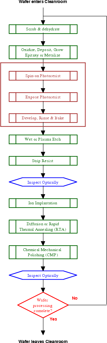
2 5 Fabrication
How a semiconductor wafer is made Process Flow.

. Mie Fujitsu semiconductor undertakes wafer processing as a foundry company to manufacture semiconductor. 1 Wafer Sawing To cut countless densely arranged chips from the wafer we must first grind the back of the wafer until. 251 Description of Semiconductor Manufacturing Processes.
Wafer fabrication process flow wafer fabrication process and measurement tools wafer fabrication process chemistry andphysics reliability physics and defect generation and. Develop a Step-by-Step Visual Guide to Different Processes. The process flow is shown in Figure 46.
2 Single Wafer Attachment After all the chips are. Back EndBE Process Wafer Back Grinding The typical wafer supplied from wafer fab is 600 to 750μm thick. Develop a Step-by-Step Visual Guide to Different Processes.
It starts with a CMOS wafer. The polished starting wafers come into fabrication with blank. Silicon single crystal and silicon wafers.
Know your wafer. 14 Wafer fabrication 141 Wafer separation and surface refinement At first the single crystal is turned to a desired diameter and then bedight with one or two flats. Ad Search Thousands of Catalogs for Wafer Fabrication Processes.
Process Flow Chart Bumping Wafer is cleaned before each individual process step Photoresist Masking. The fabrication process is foundry CMOS compatible Zhao and Hua 2004. Here are a number of highest rated Wafer Fabrication Process Flow pictures on internet.
Photoresist Spinning and Baking Mask Alignment and Exposure. Each part of a finished wafer has a different name and function. The fabrication process is foundry CMOS compatible Zhao and Hua 2004.
In the manufacturing process of IC electronic circuits with components such as transistors are formed on the surface of a silicon. The first step is to define the MEMS structure. Wafer fabrication is the manufacturing processes used to create the semiconductor devices in and on the wafer surface.
Ad Gold Copper Nickel IndiumTinLead Lead-Free. Lets go over them one by one. The first step is to define the MEMS structure.
Invite Your Teammates to Join the Board. Ad Fully Customizable Premade Flowchart Template. Wafer manufacturing process flow.
Get A Free Quote Today. The process flow is shown in Figure 46. The four major process flows of wafer manufacturing.
1Silicon Manufacturing a Czochralski method. Wafer thinned down to the required thickness 50um to. Wafer Fabrication Process Flow.
Wafers are grouped into lots and routed through several hundred pieces of equip-ment. Invite Your Teammates to Join the Board. FEOL Front End of Line.
Wafer thinning is implemented during different process steps as the wafer moves into the manufacturing process flow. It starts with a CMOS wafer. Semiconductor Manufacturing Process Fundamental Processing Steps.
Ad Use Our Wafer Processing Devices For An Efficient Wafer Processing Solution. We identified it from honorable source. Ad Fully Customizable Premade Flowchart Template.
After the ingot first gets sliced into the individual wafer. Enjoy Reliable Support From Our World Class Team Of Experts. A tiny piece of silicon with electronic circuit patterns.
B Wafer Manufacturing c. The larger first flat.

Basic Semiconductor Manufacturing Process

The Process Of Fabrication 1 Silicon Wafer Pretreatment To Maintain Download Scientific Diagram
Improving The Sic Wafer Process Power Electronics News
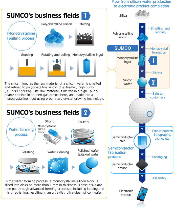
What Is Silicon Wafer Sumco Corporation